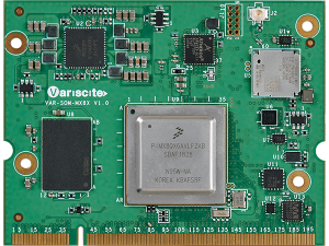
After designing and building a custom carrier board based on a Variscite i.MX System on Module / Computer on Module, one of the first tasks for your software team will be to create a new device tree file for the Linux kernel. The device tree is responsible for describing the hardware configuration to the kernel, including the function and settings of each pin. Most i.MX SoC pins are multiplexed and offer up to 8 alternate pin functions. Additionally, most pins have configurable settings such as internal pull-ups, pull-downs, etc. This guide walks through how to configure a pin function and its settings for devices in the Linux device tree for Variscite i.MX System on Modules.
Setting up the pinmux for a device
When adding a device node that requires physical control over a pin, such as I2C, PWM, UART, etc. it is necessary to specify the function and settings for each pin. There are two main steps to this:
- Add a pin group node to the iomuxc node that defines the pin function and settings
- Reference that pin group node in the node of the new device that you are adding
To demonstrate this process, let’s review the pinmux configuration for UART3 on the VAR-SOM-MX8X SoM:
Step 1: Add a pin group node to the iomuxc node
For VAR‑SOM‑MX8X, The UART3 pin group node is defined in imx8qxp-var-som.dtsi:
&iomuxc {
…
pinctrl_lpuart3: lpuart3grp {
fsl,pins = <
IMX8QXP_SCU_GPIO0_00_ADMA_UART3_RX 0x06000020
IMX8QXP_SCU_GPIO0_01_ADMA_UART3_TX 0x06000020
>;
};
};
iomuxc is a device node for the imx8qxp pinctrl driver. It is defined in imx8qxp.dtsi. Documentation for this node can be found in the Linux kernel source tree, at:
Documentation/devicetree/bindings/arm/freescale/fsl,scu.txt
Documentation/devicetree/bindings/pinctrl/fsl,imx-pinctrl.txt
pinctrl_lpuart3 is a label used to provide a name for the UART3 pin group. We will use this label in the next step.
“fsl,pins” is a list of pins used on UART3 and their configuration. Each entry consists of a macro for the pin function (pinmux) and an integer for the pad setting (internal pull-ups, pull-downs, etc.).
Pin Function:
Each pin has up to 8 functions that are multiplexed. To simplify selecting the pin function, NXP provides macros for each SOC with the following naming convention:
<SOC>_<PIN NAME>_<PIN FUNCTION>
In this example, the “fsl,pins” has two pin entries: pin SCU_GPIO0_00 is configured for function ADMA_UART3_RX and pin SCU_GPIO0_01 is configured for function ADMA_UART3_TX.
Warning: To avoid pinmux conflicts, each pin should be set to just one function and each function should be assigned to just one pin.
Each i.MX SoC has a pin config file with pin function macro definitions as well as documentation in the device tree bindings directory. For more information about the values of the pin function macros, please refer to the documentation of the specific SoC.
For i.MX8X and i.MX8QM, the pin header files are located at “include/dt‑bindings/pinctrl/” and as mentioned before, the documentation is located at “Documentation/devicetree/bindings/arm/freescale/”
| Header file | Documentation |
| pads-imx8qxp.h | fsl,scu.txt |
| pads-imx8qm.h | fsl,scu.txt |
For the i.MX8M family, the pinfunc files are located at “arch/arm64/boot/dts/freescale/” and the documentation is located at “Documentation/devicetree/bindings/pinctrl/”
| Header file | Documentation |
| imx8mp-pinfunc.h | fsl,imx8mp-pinctrl.txt |
| imx8mq-pinfunc.h | fsl,imx8mq-pinctrl.txt |
| imx8mm-pinfunc.h | fsl,imx8mm-pinctrl.txt |
| imx8mn-pinfunc.h | fsl,imx8mn-pinctrl.txt |
For the i.MX6/i.MX6UL/i.MX7 families, the pinfunc files are located at “arch/arm/boot/dts/” and the documentation is located at “Documentation/devicetree/bindings/pinctrl/”
| Header file | Documentation |
| imx6dl-pinfunc.h | fsl,imx6dl-pinctrl.txt |
| imx6q-pinfunc.h | fsl,imx6q-pinctrl.txt |
| imx6ul-pinfunc.h | fsl,imx6ul-pinctrl.txt |
| imx6ull-pinfunc.h | fsl,imx6ul-pinctrl.txt |
| imx7d-pinfunc.h | fsl,imx7d-pinctrl.txt |
Pad Setting:
In addition to the pin function macro, each “fsl,pins” entry requires a value for the pad settings. In this case, 0x06000020 is the pad setting value that configures the pin pull-up, drive strength, etc. The configuration options for each pin are described in the i.MX8QXP Reference Manual.
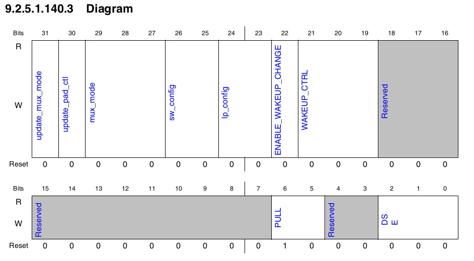
Below is the pad/mux control register for the UART3_RX pin, from the i.MX8QXP Reference Manual Rev. 0, 05/2020, page 957:

Figure 1: Pad/mux control register for SCU_GPIO0_00

| Field | Function |
| 31 update_mux_mode |
update lock for mux control write 1 to allow programming to mux control [29:19] |
| 30 update_pad_ctl |
update lock for pad control write 1 to allow programming to pad control [14-1:0] |
| 29-27 mux_mode |
mux_mode 000b – SCU_GPIO0_IO00 001b – SCU_UART0_RX 010b – M40_UART0_RX 011b – ADMA_UART3_RX 100b – LSIO_GPIO2_IO03 |
| 26-25 sw_config |
output and input configuration 00b – DEFAULT 01b – OPEN_DRAIN 10b – OPEN_DRAIN_INPUT 11b – INOUT |
| 24-23 lp_config |
lower power configuration 00b – PASS 01b – EARLY_ISO 10b – LATE_ISO 11b – LATCH |
| 22 ENABLE_WAKEUP_CHANGE |
Enable WAKEUP change Allows modification of the WAKEUP_CTRL field without having to read or modify the other bits |
| 21-19 WAKEUP_CTRL |
wakeup control 000b – OFF 001b – RESAMPLE (The wakeup field is not modified (it retains its old value) but because a write is done, the flag is cleared) 100b – LOW 101b – FALL 110b – RISE 111b – HIGH |
| 18-17 | Reserved |
| 6-5 PULL |
Pull Down Pull Up 00b – Bus-Keeper 01b – pull up 10b – pull down 11b – No Pull |
| 4-3 | Reserved |
| 2-0 DSE |
Drive 000b – Drive select 1mA 001b – Drive select 2mA 010b – Drive select 4mA 011b – Drive select 6mA 100b – Drive select 8mA 101b – Drive select 10mA 110b – Drive select 12mA 111b – High Speed |
Considering this register has the value of 0x06000020 (bits 5, 25, 26 enabled) in this example, this is the list of all configurations and their values:
update_mux_mode: value 0
update_pad_ctl: value 0
mux_mode: value 0 (Configured by the pin function macro)
sw_config: value 0b11
lp_config: value 0
enable_wakeup_change: value 0
wakeup_ctrl: value 0
pull: value 0b01: Internal pull up resistor selected.
DSE: value 0b000: Drive Strength of 1mA selected.
To know more about all possible configurations, please check the i.MX8QXP Reference Manual.
Step 2: Reference that pin group node in the device node
After adding the pin group node (lpuart3grp) to iomuxc, the next step is to provide a reference to the device node that will use these pins. In this example, this is lpuart3, which is defined in imx8-ss-dma.dtsi and configured by Variscite in imx8qxp-var-som-symphony.dtsi:
/* Console */
&lpuart3 {
pinctrl-names = “default”;
pinctrl-0 = <&pinctrl_lpuart3>;
…
};
During lpuart3 initialization, the Linux device core will call pinctrl_bind_pins prior to calling the probe function in the lpuart3 driver. The pinctrl driver will then write to the i.MX specific registers to configure the default pin state for each entry in pinctrl_lpuart3.
Pin States
Some devices support multiple pin states.
For example, an MMC device:
&usdhc1 {
pinctrl-names = “default”, “state_100mhz”, “state_200mhz”;
pinctrl-0 = <&pinctrl_usdhc1>;
pinctrl-1 = <&pinctrl_usdhc1_100mhz>;
pinctrl-2 = <&pinctrl_usdhc1_200mhz>;
…
};
In this example, usdhc1 has three pinctrl states: default, 100mhz, and 200mhz. The Linux device core will initialize the default state before calling the platform driver probe function. However, the driver also has the option to change pin settings depending on the MMC mode.
For more information on this subject, see the following documentation file in the kernel source tree: “Documentation/devicetree/bindings/pinctrl/pinctrl-bindings.txt”
Summary
In summary, device nodes that need pin configuration require a reference to a pin group node defined in iomuxc. The pin group node defines the pin function and settings for each relevant pin. To learn more about the details for each SoC, the documentation is available in the kernel source tree at “Documentation/devicetree/bindings/pinctrl/”.


 Join RSS Feed


